- Published 6 Jan 2023
- Last Modified 8 Jan 2024
- 9 min
Choosing the Right Development Boards & Tools

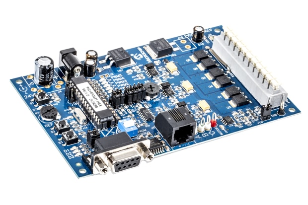
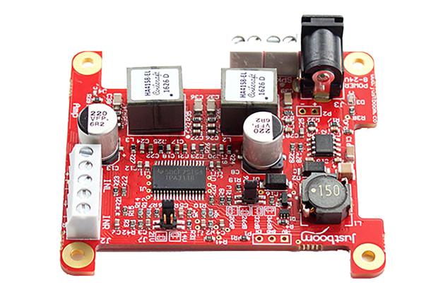
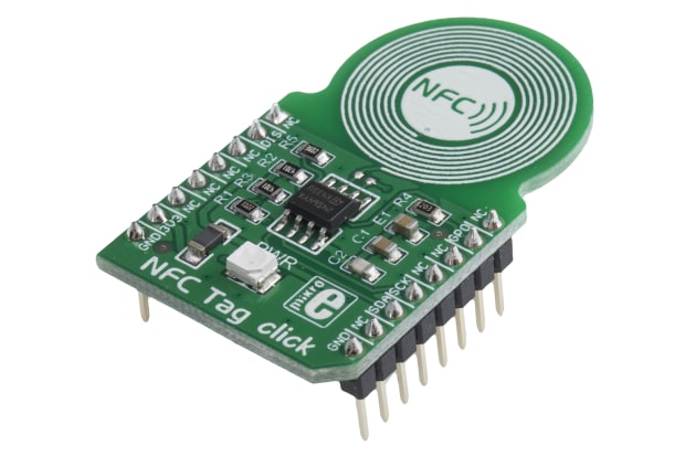
Development boards and tools exist to help engineers create electronics projects at home or to test and improve established systems and programs. This guide provides an overview of some popular types of dev tools and boards, to help you to decide what is best for you - from the more advanced, to simpler boards with the necessary clock circuitry.
The Advantages of Using Development Systems
Many engineers prefer not to use development environments, instead preferring to embed debug points into their code and use test equipment to validate their hardware. However, there are distinct advantages to using a development tool, and they fall roughly into three areas
- Parallel engineering
- Time to market improvements
- Known good circuitry
Parallel Engineering is probably the simplest of these. Many projects have multiple engineers working on them, and it’s great when, for example, the software engineer, is able to start testing code before system PCBs are available. This is particularly true if the target board requires complex packages such as BGA which cannot be easily bread-boarded, or perhaps the circuit requires a long lead time element such as an ASIC. Additionally, of course, it’s possible to use multiples boards to compare and contrast different products without the need to invest hugely in tools for testing. Parallel engineering saves time and resources, which means faster time to market.
Time to market is an important parameter in engineering, and can often determine the commercial success or failure of a product. So how does a development tool help with this? The answer is multiple: first, many development kits, particularly in the MCU arena, come with productivity tools as part of the package. Examples of these tools are ready written device drivers for peripherals, and/or the porting of a real time operating system for a given device. This means coding (often the major determinant in a project timescale) can be accelerated and it becomes more deterministic, so can lead to reduced chances of a product recall.
Another area that development boards can speed development is where the supplier provides circuit layout details such as Gerber files. This can be critical in analogue or high-speed systems. Access to information that can be studied, or in the final analysis, copied, can save many hours of hard labor and more importantly, multiple PCB iterations.
Finally, the known good circuit. Many of us have been in the situation where we have with all due diligence gone to the ‘final’ PCB stage and yet have encountered an intermittent bug somewhere in the system. Having a known working board can be useful in finding those often frustrating issues. An example of this is an occasional instability in a switching power supply feedback circuit caused by higher than calculated parasitic capacitance in the layout. An inspection of the evaluation board Gerber files can be extremely helpful in isolating this problem before the final stage.
Evaluation Boards
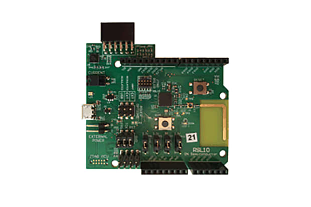
Often included in the generic terminology of development tools, these boards are supplied by silicon manufacturers, as a way of allowing customers to appraise benefit for the application, without the inconvenience of a breadboard or PCB. Usually these are relatively simple boards, supplied with sufficient software (where necessary) or ancillary components to check out functionality and usability. While not primarily intended as a development board in many cases they have sufficient on-board resources and can be used this way.
Obviously if you are evaluating a programmable device such as a microcontroller, then evaluation boards can be used for coding and many come with freeware compilers and debuggers sufficient for completing a smaller application. It is worth noting that many suppliers are moving towards equipping their boards to interface with standard development boards like Arduino, (these are known as shields). To allow ease of use many manufacturers give their own boards an Arduino compatible i/o system to allow users access to the variety of shields in the world. The release of this standard has spawned a complete ecosystem of shields from other suppliers allowing quite sophisticated systems to be constructed.
Manufacturer Development (or Demonstration) Boards
Manufacturer supplied development tools generally come equipped with a higher compliment of resources than an evaluation board. This is especially true for parts aimed at tightly defined applications. In these cases, manufacturers will equip the board with all of the components that they deem fit to implement into the target application. As an illustration, let’s take a supplier targeting an automotive dashboard application, it is likely the board will be equipped with an MCU, CAN controller/interface, a display of some kind and a robust power supply design at the bare minimum. Even if the additional parts seem extraneous, they can still be extremely useful for development purposes. Manufacturers are practical enough to fit their boards with expansion capabilities, or at the very least access to I/O, so non-specific development is still possible even on tightly focussed boards. Positively, many supplier development systems are designed as general-purpose tools and come with a good range of coding and debugging software
When discussing supplier initiated development tools, one other term that is often encountered is ‘reference design’. These tend to be tightly focused on a single application, and unlike development boards, they are likely to have been cost/power or space optimised and are less accessible to general use (although of course very useful if you are seeking to design a product in the focused area). Their advantage that they are optimised and thoroughly tested to give great insight into the design rules to be followed.
STM Nucleo boards
As an example of the variety of development tools that are available, we’ll take a quick look at the ST Micro Nucleo boards. These boards are a much-focused manufacturer board released to support their STM32 MCUs. They support the major toolchain suppliers and their own tools, but most interestingly they are MBED compliant, support the various Arduino pinouts, and allow access to both ST’s and third party shields, giving you lots of options. Other suppliers are moving in this direction and increasing the sophistication and depth of coverage of their tools by addressing the standardised I/O regimes.
Third party development tools
The majority of third-party tools tend to be focussed on the microcontroller market. These typically make use of the manufacturers on chip emulation systems based on JTAG. These allow the development tool to ‘get inside’ the MCU noninvasively and allow the users to set break points; trace code paths; and, examine internal memory content. They typically come with a ‘C’ or ‘C++’ compiler and a debug system known as an Integrated Development Environment or ‘IDE’. The IDE allows you access to the executing software at a high level of abstraction which is a far cry from the assembler code of old. This means you have access to global/local variables and can evaluate the content of arrays and structures of variable data types, etc. Additionally, they also allow access to low-level code, I/O, and board-level hardware, some even come close to logic analyser capabilities. All of this is, of course, essential when debugging the complex real-time systems implemented in many embedded designs.
There are many sources of third party boards, varying from compiler suppliers providing target boards for their toolchains; through to in-circuit emulator manufacturers; and, companies addressing the ecosystems mentioned earlier. This leads to a rich variety of options for you, covering a wide range of price points and system complexity.
MBED based tools and boards
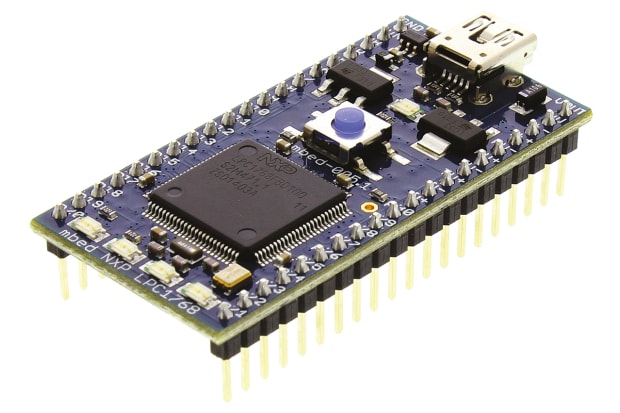
MBED is a development system provided by ARM holdings, and not surprisingly is targeted at their processor cores. It’s particularly of interest if you are developing products accessing Internet of Things (IoT) systems, and offers a full suite of useful communications and security libraries as well the usual IDE, RTOS (and small Linux) and compilers. Unlike many other suppliers the tools set resides in the cloud and development is done via the MBED servers, although an offline variant is possible, and code can be run on the users own hardware. Although primarily targeted at IOT edge products, it is perfectly useable for other systems and has a vast library of community and ARM generated software to use.
Where MBED differs from other offerings is that it relies on third parties to provide hardware targets. Suppliers of these boards (often semiconductor companies such as NXP and STMicro) have to ensure their modules, boards and chips are compliant with the MBED test suite. In general, all manufacturing details, source code etc. is freely available, and boards are equipped with the approved MBED pinouts.
Summary
When evaluating the hundreds of tools that are available, the choice tends to come down to multiple key points:
- Budgetary constraints - tools cost from a few dollars to tens of thousand
- Complexity of the system being designed – do you need a fully featured solution
- Familiarity with the development tool chain –
- Sophistication of the tool chain-such as code density of the compiler, availability of device drivers and so on
- Collaboration - ability to support multiple users in a development team.
- Freeware or Licensed – can you use freeware or do you need to go to licensed software and the associated support costs
All of these decision points can lead to an extended evaluation phase, but getting the decision right at the beginning can lead to a shortened design lifecycle and faster speed to market. Today’s engineers are fortunate in the number and variety of development tools that are available for them to choose between. However, this profusion of options can be a challenge in itself. One thing is for sure though, selecting the right tools can save many weeks of development time in a project, and for that reason a careful examination of the options is advisable.
Related Product Categories
Use the links below to browse related products.
Related links
- STMicroelectronics STM32 Nucleo-64 MCU Development Board NUCLEO-F401RE
- Microcontroller Development Tools
- STMicroelectronics X-Nucleo-IHM Stepper Motor Driver for L6208 for...
- STMicroelectronics X-Nucleo-IHM Stepper Motor Driver for STM32...
- Microchip EV48R50A, Graphics Prototype Board For Curiosity Boards...
- Sparkfun Development Boards ESP8266 Development Board for Baby...
- Wurth Elektronik Calypso WiFi FeatherWing WiFi Development Kit for...
- Wurth Elektronik Thyone-I Wireless FeatherWing Development Kit for...
