- Published 17 Jan 2023
- Last Modified 5 Apr 2024
- 5 min
Energy Harvesting: Operating a Wireless Switch

Published January 2022
Energy harvesting is the extraction of small amounts of electrical energy from sources such as ambient light, temperature gradients, vibrations and electromagnetic radiation. Ultra-low-power solutions can use this energy to operate devices autonomously.
Everyday objects of this genre include calculators and clocks powered by a solar cell. Unfortunately, the energy format that harvesters provide is usually of little use for operating electronics. Sometimes the voltage is too low, sometimes too high, and sometimes it is a random type of alternating voltage. This article shows how a wireless sensor solution – in this case, a switch with very low power consumption – can be powered from variable voltage and current states.

We want to turn on a light without having to lay a cable between the switch and the light fitting. This on/off signal is to be transmitted wirelessly. We don’t know which component is intended for this. What we do know is that it requires a supply voltage of 1.8V.
The energy harvester we are using is the AFIG device (Fig. 1; right) from ZF, which, in its end application, can signal commands via Bluetooth 5 (RSL10 SIP from onsemi).
The harvesting concept is shown in Fig. 2. When the switch is actuated, a permanent magnet is moved, which generates a field change in the coils and creates a current flow. The electrical energy yield of a switching operation at a load of 100Ω is about 0.33mWs; the peak voltage is between 6V and 15V.
Fig. 2
When the switch is actuated, a permanent magnet is moved, which generates a field change in the coils and creates a current flow.
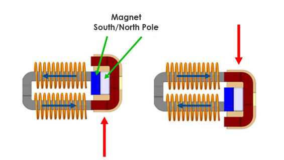
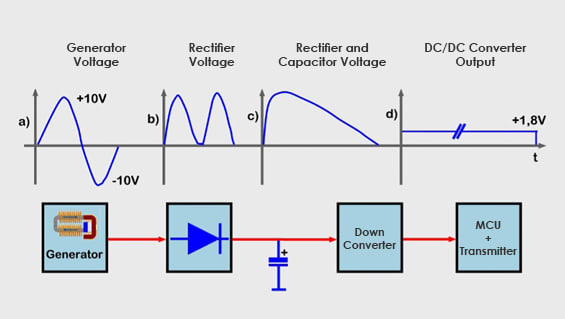
Fig. 3 shows the signal shapes of the harvester's output voltage at the different stages of power management. During the switching operation, the switch outputs an AC voltage. However, control and transmission electronics cannot work with this. With the help of a diode, a pulsating positive voltage is generated in the next step. A capacitive sensor smooths out the waveform and provides the voltage curve c). This voltage still cannot be used to operate a transmitter/receiver chip.
Wireless sensor solutions with very low power consumption require a power management device because of their variable voltage and current states. This component converts the delivered unregulated voltages and currents into regulated electrical energy that can be stored. It can also pass energy (as in this example) to the system load at the correct voltage. Typically, the power management chip contains circuits to protect both the load and any energy storage devices that may be present.
In this example, the TPS62125 is used as a DC converter. A down-converter from Texas Instruments generates the e.g. 1.8V we need to operate of RF part.
Fig. 3
Signal shapes of the harvester's output voltage at the different stages of power management.
The component has a wide input voltage range of up to 17V and operates on a quiescent current or IQ of about 11µA. The latter is an important parameter because it indicates the proportion of electricity that is not available for useful electronics.
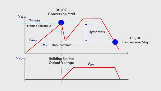
A special feature of the 62125 is an input voltage monitoring device in the shape of a comparator unit that switches the component on and off. This SVS (Supply Voltage Supervisor) is important in energy harvesting applications to ensure a reliable and clean start to the voltage conversion. With the TPS 62125, the switch-on/switch-off voltage of the comparator can be adjusted with resistors. So, when the input voltage rises after actuating the light switch, it reaches the threshold where the DC/DC converter turns on and the output voltage begins to increase. The converter provides a stable output voltage as long as the input voltage has not reached the lower switching threshold (the switch-off threshold).
A certain inrush current is always drawn when the converter is started. This leads to a drop in the input voltage, as not all the energy has been harvested at this point. There may be problems with starting the DC converter properly. This is avoided when the capacity is loaded in the supply path.
Fig. 4
Input voltage monitoring of the DC/DC converter using a comparator that switches the component on and off.
Setting the TPS62125
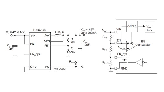
Fig. 5 shows a typical application of the TPS62125. An output voltage of 3.3V is set and the comparator is not configured. The output voltage is programmed with the potential divider R1 and R2. Table 1 (below) lists the resistance values for selected voltages.
Output Voltage | 1.2V | 1.8V | 3.3V | 5V | 6.7V | 8V |
|---|---|---|---|---|---|---|
| R1 (kΩ) | 180 | 300 | 1800 | 1100 | 1475 | 1800 |
| R2 (kΩ) | 360 | 240 | 576 | 210 | 200 | 200 |
Fig. 5
A typical application of the TPS62125 (left). An output voltage of 3.3V is set and the comparator is not configured. The comparator is set up with three resistors (right).
Images: Texas Instruments
If you want to try your hand at it yourself, here are the formulas:

The comparator (Fig. 4) is set up with three resistors (Fig. 5 on the right). The input voltage level VIN start-up at which the converter starts can be set and calculated by resistors REN1 and REN2 by:

Resistance values REN1 and REN2 result from:

The switch-off level from which the converter stops working is determined with resistors REN1, REN2 and REN hys:

Where REN hys is made up of:

The current through resistors REN1, REN2 and REN hys should be greater than 1µA. In applications where the converter is operated over the entire temperature range, the resistance values can be reduced to smaller values.
Where to Next?
Related links
- Batteries Not Included: Wireless Sensor Solutions
- onsemi Energy Harvesting Bluetooth Low Energy Switch RSL10 SIP Bluetooth Development Kit for NCH-RSL10-101S51-ACG,
- Energy Harvesting for IoT Devices
- Wurth Elektronik EFM32 Gecko Energy Harvesting
- MikroElektronika Qi Receiver Click Energy Harvesting Add On Board MIKROE-2799
- STMicroelectronics Battery Charger, Energy Harvesting for SPV1050
- STMicroelectronics Evaluation Kit Energy Harvesting for SPV1050 for Power Converter
- Schneider Electric 630A 3.7W, Wireless

