- Published 17 Jan 2023
- Last Modified 25 Jan 2024
- 16 min
A Complete Guide to MOSFET Transistors
Learn everything you need to know about MOSFETs in our complete guide and discover leading brands and products.

MOSFETs are among the most popular types of transistors thanks to their versatility and widespread use. In this guide, we will explain how these transistors work as well as sharing practical tips for using MOSFETs and choosing the most suitable type of MOSFET.
Primary Types of Transistor
There are two primary types of transistors. The first is the Bipolar Junction Transistor (BJT) and the second is the Field Effect Transistor (FET). MOSFETs are a type of FET. BJTs are usually used for electrical currents of under one amp, while MOSFETs are typically used for higher-current applications.
Users can choose between MOSFETs featuring depletion or enhancement modes. The depletion mode operates in a similar way to the closed switch, with current flowing when the on voltage is applied. If a negative voltage is applied, then the current will stop. On the flip side, enhancement mode MOSFETs are the most commonly used type for modern-day applications.
What is a MOSFET Transistor?
The Metal Oxide Semiconductor Field Effect Transistor (MOSFET) is a commonly used semiconductor in digital and analogue circuits and is also a useful power device. As the original compact transistor, it is suitable for a wide variety of electrical applications.
It has been argued that many of the 21st century’s technological developments wouldn’t have been possible without the MOSFET. It is more widely used than the BJT as it requires minimal current for load-current control. The level of conductivity can be increased from the ‘normally off’ state when the MOSFET is set to enhancement mode. Voltage transmitted via the gate can minimise conductivity from the ‘normally on’ state. The process of miniaturising MOSFETs is relatively simple and they can be effectively scaled down for compact applications.
Additional advantages of the MOSFET include rapid switching (particularly in relation to digital signals), minimal power consumption, and high-density capacity which makes them ideally suited to large-scale integration.
The MOSFET is a core component of the integrated circuit and it can be designed and fabricated in a single chip due to its compact size. It features four terminals, these being the Source (S), Gate (G), Drain (D), and Body (B). The body is typically connected to the source terminal so that the MOSFET functions as a field-effect transistor.
How Do MOSFETs Work and What Do They Do?
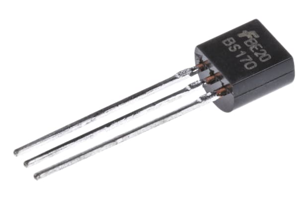
MOSFETs feature three pins - Source, Gate and Drain. They effectively control the electrical current flowing between the Source and Drain contacts, with voltage being applied via the Gate. You can prompt the appearance or disappearance of an electrical channel by altering the electrical voltage. This enables the electrical device to be switched on or off. The use of a semiconductor allows for the separation of different impurity varieties. This means that charges of different signs can be effectively isolated, and barriers can be created, preventing the flow of charge from one region to the next.
The transfer of current from the Gate to the Source terminals will result in current flowing from the Drain to the Source pins. The Drain-source resistance will ideally be very high when there is no current flowing and low when the current is transmitted. However, you should be aware that MOSFETs complete with microcontrollers may require 10-15 Gate Source potential difference for the lowest level of Drain source resistance with the microcontroller operating on 5v or 3.3v.
The MOSFET Gate source pins have a capacitance that prevents rapid switching between states. High current will be necessary for a rapid change between voltage on internal capacitance. It must prompt an automatic switch between the change (source) and discharge (sink). A change in voltage applied to the Gate will result in a simultaneous switch in resistance from the Drain to the Source. The levels of voltage will correspond directly with the levels of resistance. Power MOSFETs are purpose-made for applications involving the generation of high power levels.
Different Types of MOSFET Transistors
PMOS Logic
As previously mentioned, the integration of a MOSFET allows for high levels of circuit efficiency when compared with BJTs. P-channel MOSFETs can be used with PMOS logic to implement digital circuitry and logic gates.
NMOS Logic
NMOS logic is similar to PMOS logic with the exception that N-channel MOSFETs are applied to logic gates and related digital circuitry. As a general rule, N-channel MOSFETs can be smaller than P-channel MOSFETs which makes them more attractive in certain situations. However, NMOS logic constantly consumes power whereas PMOS logic does not.
CMOS Logic
Complementary metal-oxide-semiconductor (CMOS) logic is a technology used to produce integrated circuits. Such circuits are featured across a range of electrical components and are known to generate electrical power. Both P and N-channel MOSFETs are used in conjunction with connected gates and drains in order to reduce power consumption and excess heat generation.
Depletion Mode MOSFET Devices
Depletion mode MOSFET devices are among the less common types of MOSFETs. They have a low channel resistance, with the channel being considered as ‘ON’. When set to the no-power state these switches will conduct in accordance with their design. The channel resistance will be linear, with low distortion across the signal amplitude range.
MISFETs
All MOSFETs are MISFETs (Metal Insulator Semiconductor Field Effect Transistors) but not all MISFETs are MOSFETs. The gate dialectic insulator featured in this type of component is silicon dioxide in a MOSFET, however, alternative materials can be used. The gate dialectic is positioned underneath the gate electrode and above the MISFET channel.
Floating-Gate MOSFETs (FGMOS)
The floating-gate MOSFET features an electronically isolated gate. This has the effect of generating a floating node in DC together with a range of secondary gate inputs situated above the floating gate. Among various other uses, the FGMOS is typically used as a floating-gate memory cell.
Power MOSFETs
The structure of the power MOSFET is vertical, rather than planar. This allows the transistor to maintain high blocking voltage and high current simultaneously. The transistor voltage rating corresponds directly to the doping and thickness of the N-epitaxial layer, with the current rating being a result of the channel width. There is also a direct link between the component area and level of current that can be sustained by this type of device. The power MOSFET allows for low gate drive functionality, rapid switching speed, and advanced paralleling capabilities.
DMOS
These double-diffused metal oxide semiconductors come in lateral and vertical varieties. The majority of power MOSFETs are constructed using this kind of technology.
MOS Capacitors
This type of capacitator has the MOSFET structure, with the MOS capacitator being flanked by dual P-N junctions. It is typically used as a memory chip storage capacitator and support for the charge-coupled device (CCD) in image sensor technology.
TFT
The thin-film transistor (TFT) is a unique type of MOSFET. Creating this variety involves the deposition of thin semiconductor films, combined with a dialectic layer and metallic contacts over a supporting substrate. A range of semiconductor materials may be used, with silicone being a common variety. They can be made to be completely transparent and are used in the manufacture of video display panels.
Bipolar-MOS Transistors
The BiCMOS is an integrated circuit featuring BJT and CMOS transistors on a single chip. The insulated-gate bipolar transistor (IGBT) has similar functionality to the MOSFET and bipolar junction transistor (BJT).
MOS Sensors
A range of MOS sensors has been developed to accurately measure physical, chemical, biological, and environmental variables. Examples include the open-gate FET (OGFET), ion-sensitive field-effect transistor (ISFET), gas sensor FET, charge flow transistor (CFT), and enzyme-modified FET. Commonly used sensors used for digital imaging include the couple-charged device (CCD) and active-pixel sensor (CMOS sensor).
Multi-Gate Field Effect Transistors
The dual-gate MOSFET has a tetrode configuration, with the level of current being controlled by the two gates. It is typically used for small-signal devices in radio frequency applications that call for the reduction of gain loss associated with the Miller effect. This effect occurs when separate transistors are replaced in a cascode configuration.
RHBD
It is quite common for the enclosed-layout transistor (ELT) to be used to create a radiation hardened by design (RHBD) device. The gate of the MOSFET typically surrounds the drain, which is situated close to the centre of the ELT. The source of the MOSFET surrounds the gate in this instance. The H-gate is another type of MOSFET which ensures minimal radiation leakage.
MOSFET Applications and Uses
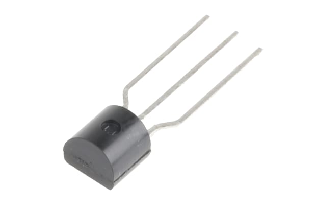
As previously mentioned, the MOSFET is a device used to switch or amplify electrical signals. This is achieved through alteration of the conductivity in relation to the level of the applied voltage.
The MOSFET is the most common transistor in digital circuits, with the potential for millions being integrated into a memory chip or microprocessor. MOSFET transistors are also commonly included as voltage-controlled circuit switches. It is thought that the development of technologies such as the pocket calculator and digital wristwatch wouldn’t have been possible without the MOSFET.
MOS Integrated Circuits
The MOSFET is the most popular type of transistor and is essential for the electrical operation of integrated circuit (IC) chips. They do not require the same series of steps as bipolar transistors for P-N junction isolation on a chip. However, they do allow for relatively easy separation.
CMOS Circuits
A complementary metal-oxide-semiconductor is a form of technology used to develop integrated circuits. Such technology is used in the manufacture of integrated circuit (IC) chips such as microprocessors, microcontrollers, memory chips and other digital logic circuits. It is also a primary component in the development of analogue circuits including image sensors, data converters, RF circuits, and integrated transmitters for digital communication.
The key characteristics of CMOS devices include high noise immunity and minimal static power consumption. Such devices produce minimal excess heat when compared with alternative forms of logic such as the NMOS logic or transistor-transistor logic. Such characteristics allow for the integration of high-density chip logic functions.
Analogue Switches
The benefits of MOSFETs for digital circuit integration far outweigh those for analogue integration. The transistor behaviour is different in each instance. Digital circuits can be switched fully on or off for the majority of the time. The level of speed and charge are the two primary factors which have a bearing on the switching process. Functionality must be ensured in the transition region of the analogue circuit in the event that minor V changes can alter the output (drain) current.
MOSFETs are still integrated across a variety of analogue circuits because of the associated advantages. Such advantages include reliability, zero gate current, and high and adjustable output impedance. There is also the potential for changing the characteristics and performance of analogue circuits through adjustments to the MOSFET size. MOSFETs are also a preferred option for switches due to the gate current (zero) and drain-source offset voltage (zero).
Power Electronics
MOSFETs are used across a broad range of power electronics. They are integrated for reverse battery protection, switching power between alternate sources, and the powering down of unrequired loads. The key features of compact MOSFETs include the small footprint, high current, and integrated ESD protection. The development of MOS technology is also widely regarded as one of the main contributing factors to the integration of network bandwidth in telecommunication networks.
MOS Memory
The development of the MOSFET allowed for the convenient use of MOS transistors for memory cell storage. MOS technology is one of the key components of DRAM (dynamic-access random memory). It offers higher levels of performance, consumes minimal power, and is relatively affordable when compared with magnetic core memory.
MOSFET Sensors
MOSFET sensors, otherwise referred to as MOS sensors, are commonly used in the measurement of physical, chemical, biological, and environmental parameters. They are also integrated within microelectromechanical systems, primarily because they allow for interaction and the processing of elements such as chemicals, light, and movement. MOS technology also has image sensing applications, being suitable for integration in charge-coupled devices and active-pixel sensors.
Quantum Physics
The quantum field-effect transistor (QFET) and quantum-well field effect transistor (QWFET) are both types of MOSFET which make use of quantum tunnelling to increase the speed of transistor operation. This is achieved by eliminating the area of electron conduction which results in the significant slowing of carriers. The operation of such quantum devices relies on the process of rapid thermal processing (RTP), using extremely fine layers of building materials.
MOSFET by Mount Types
Learn more and explore the different MOSFET mount types below.
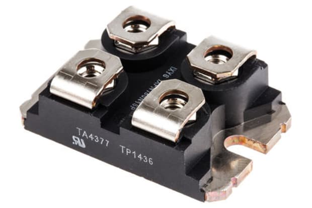
Panel Mounted MOSFETs
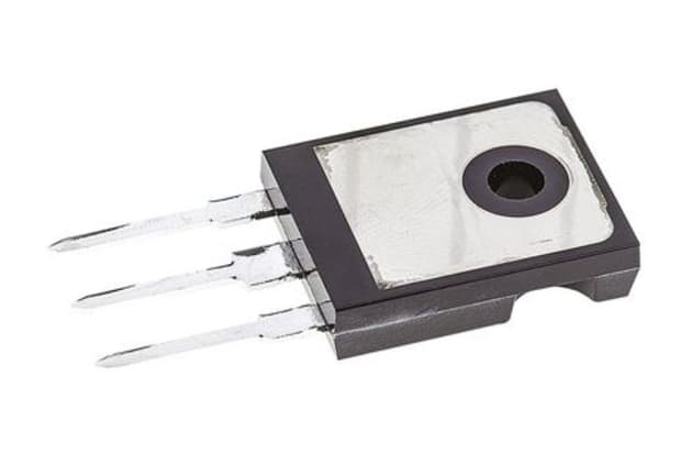
There is a wide variety of MOSFETs that can be mounted onto metal plates or heat sinks with screws. These enhancement MOSFETs allow for fast and reliable switching at high currents.
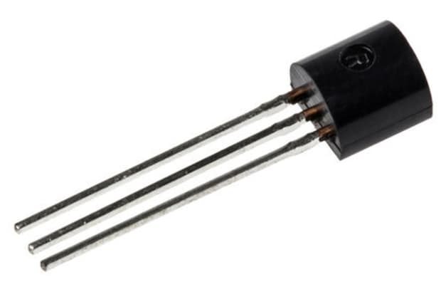
PCB Mounted MOSFETs
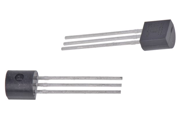
The design of the MOSFET with PCB mounting is such that the wrong fuse can’t be fitted. This form of mounting also features a tab, which prevents accidental misuse. Fuse protection is assured, and the circuits are protected against overcurrent conditions. The N-channel MOSFET is one such example, featuring a surface mount and straight lead. This MOSFET is available in tape and reel varieties. It allows for fast switching.
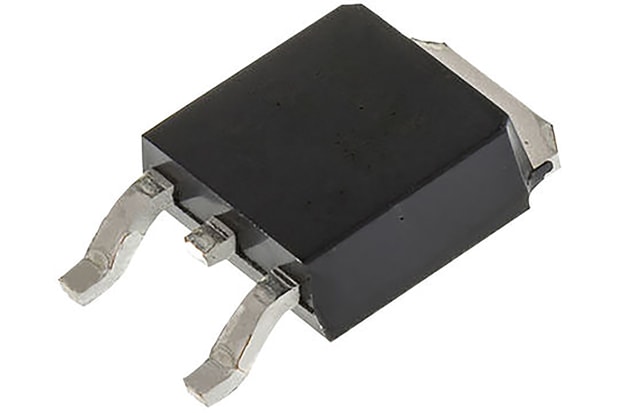
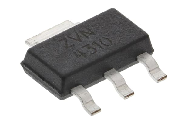
Surface Mounted MOSFETs
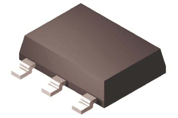
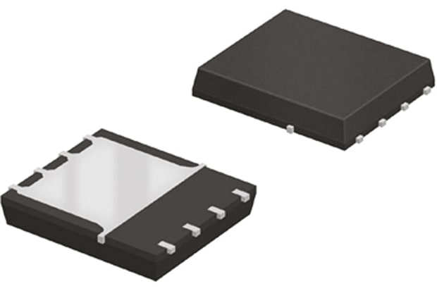
There is a great selection of MOSFETs complete with surface mounts that allow for quick and convenient PCB assembly. These compact MOSFETs are inexpensive and reliable. The N-channel ON Semiconductor MOSFET is one such example, effectively minimising on-state resistance and ensuring the reliability of switching.
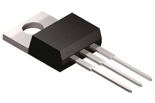
Through Hole Mounted MOSFETs
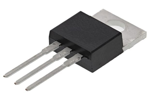
MOSFETs with through-hole mounts feature component leads, inserted into holes and securely attached to printed circuit boards (PCBs). They offer relatively strong mechanical bonds when compared to the surface-mounted variety. However, these MOSFETs are preferred for large and heavy components such as semiconductors.
What MOSFET Should I Buy?
It is essential that you select the appropriate N-channel or P-channel MOSFET for your purposes. Each of these MOSFETs functions as an electrical switch. The regular power application features a MOSFET which is connected to the ground, with the lead hooked up to the rail voltage. This is considered to be a low-side switch and requires the fitting of an N-channel MOSFET due to the levels of voltage that must be transmitted in order to switch the device on and off. The P-channel variety should be used when there is a high side switch connected to the bus and load resistor connected to the ground.
The MOSFET voltage must be taken into account. This should exceed both the rail and bus voltage to ensure sufficient protection and prevent MOSFET failure. The current rating should be of the maximum capacity for the load in all instances. Other factors that should be taken into consideration include the technology impact, thermal requirements, and switching performance. The gate parameters must also correspond with the driver circuitry. In short, the appropriate selection will depend on the application of the MOSFET.
FAQs
How Do I Test a MOSFET?
There are a number of tests that can be carried out to assess the performance of a MOSFET. First, you should check the diode drop. This will require the use of a DMM, set to diode mode. Different setups will be necessary depending on whether you are working with an N-channel or P-channel MOSFET. The ideal MOSFET reading will be 0.4V to 0.9V. However, the MOSFET will be considered defective if no voltage is generated. A resistance check should also be carried out in order to assess performance. No matter the DMM probe polarity, there should be a high resistance between the drain-source.
You can test the MOSFET with a digital multimeter as follows:
Step One: Connect the MOSFET
Connect the MOSFET source to the meter’s negative (-) lead.
Step Two: Take a Grip
Hold the tab or case of the MOSFET, while avoiding contact between the metal test probe components and terminals.
Step Three: Hook Up the Meter Positive
Attach the meter positive lead to the MOSFET gate.
Step Four: Set to Drain
Adjust the positive probe to ‘Drain’ (you should see a low reading).
Step Five: Apply Pressure
Apply a little pressure between the source and gate while the meter is positive. Ensure that the gate is discharged, resulting in a high meter reading.
How Do You Wire a MOSFET Transistor?
The required components for the wiring of a MOSFET transistor are a diode, transistor, circuit board, and wire (in three colours).
The wiring process is as follows:
Step One: Strip the Wire
Strip the wire powering the circuit.
Step Two: Insert and Secure
Insert the wire into the board.
Step Three: Connect the Power Wire
Insert the power generating wire into the device, ensuring connection with the circuit board.
Step Four: Attach the Diode
Attach the diode to the board and bridge the connection with the other power wires.
Step Five: Connect the Transistor
Fit the transistor to the board.
Step Six: Cut the Excess
Carefully remove any excess and connect the wiring.
Step Seven: Check with the Multimeter
Use a multimeter to check connections and proceed to the control of high voltage devices accordingly.
How Do You Read the Numbers on a MOSFET?
It will be necessary to correctly read the numbers of a defective MOSFET to ensure that a suitable replacement can be ordered. This will require reference to the part number and identification chart.
The number reading process is as follows:
Step One: Check the MOSFET Variety
Identify whether it is an enhancement or depletion MOSFET.
Step Two: Check the Voltage Reading
Take the voltage reading from the bottom of the transistor.
Step Three: Check the Transistor Series Number
Identify the transistor series number (as an example, the first two letters assigned to the BU series transistor are BU).
Why is a MOSFET a Voltage-Controlled Device?
This is because the output (drain) current can be controlled via the gate-source voltage. The voltage applied to the input terminal effectively controls the flow of current so that the output is directly proportional to the input voltage.
Popular Brands
Microchip
Explore the full range of Microchip MOSFETs, including a selection of products best suited to varying applications.
Fairchild
Fairchild Semiconductor offers a wide range of high-quality MOSFETs. Browse the range and shop online with RS.
Texas Instruments
Browse MOSFETs from Texas Instruments and discover the most suitable product for your requirements with RS.
Infineon
RS offers an extensive range of Infineon MOSFETs, giving you the freedom to select the most suitable product.
